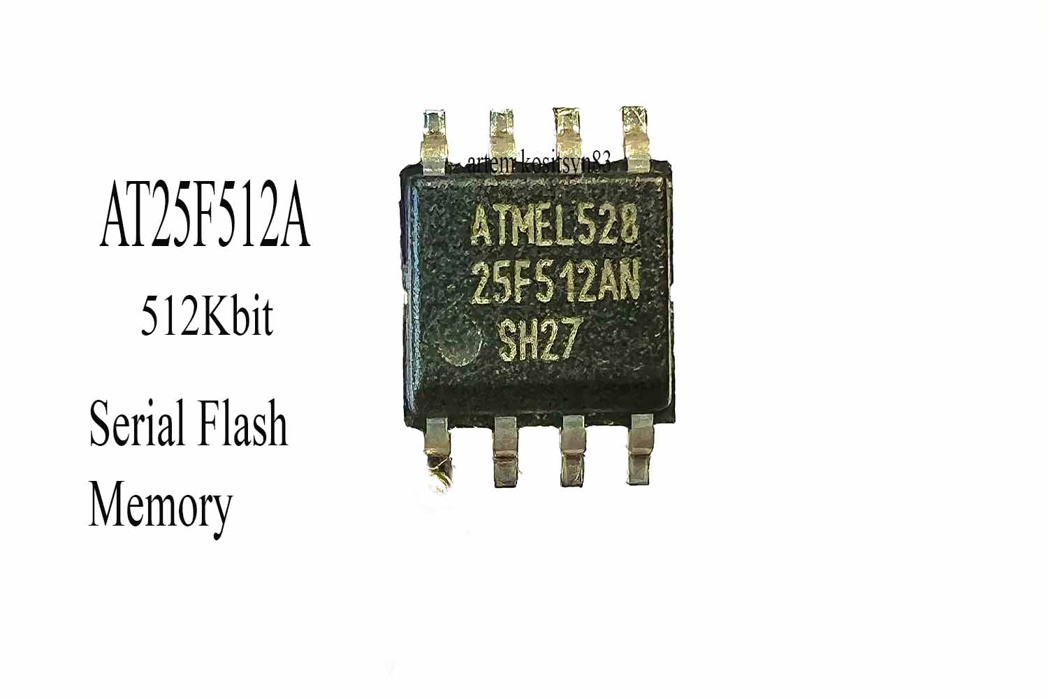
The AT25F512A provides 524,288 bits of serial reprogrammable Flash memory organized as 65,536 words of 8 bits each. The device is optimized for use in many industrial and commercial applications where low-power and low-voltage operation are essential. The AT25F512A is available in a space-saving 8-lead JEDEC SOIC and 8-lead SAP packages. The AT25F512A is enabled through the Chip Select pin (CS) and accessed via a three-wire interface consisting of Serial Data Input (SI), Serial Data Output (SO), and Serial Clock (SCK). All write cycles are completely self-timed. Block write protection for the entire memory array is enabled by programming the status register. Separate write enable and write disable instructions are provided for additional data protection. Hardware data protection is provided via the Write Protect (WP) pin to protect against inadvertent write attempts to the status register. The HOLD pin may be used to suspend any serial communication without resetting the serial sequence.
• Serial Peripheral Interface (SPI) Compatible • Supports SPI Modes 0 (0,0) and 3 (1,1) – Datasheet Describes 0 Operation • 33 MHz Clock Rate • Byte Mode and 128-byte Page Mode for Program Operations • Sector Architecture: – Two Sectors with 32K Bytes Each – 256 Pages per Sector • Product Identification Mode • Low-voltage Operation – 2.7 (VCC = 2.7 to 3.6V) • Sector Write Protection • Write Protect (WP) Pin and Write Disable Instructions for both Hardware and Software Data Protection • Self-timed Program Cycle (75 μs/byte typical) • Self-timed Sector Erase Cycle (1 second/sector typical) • Single Cycle Reprogramming (Erase and Program) for Status Register • High Reliability – Endurance: 10,000 Write Cycles Typical – Data Retention: 20 Years • 8-lead JEDEC SOIC and 8-lead SAP Packages
AT25F512A on the Seagate barracuda 7200.9 hard drive board


![Подробнее о статье MX29LV040.4M-BIT [512K x 8] CMOS SINGLE VOLTAGE.Datasheet](https://electronics83.com/wp-content/uploads/2023/11/29lv040.jpg)