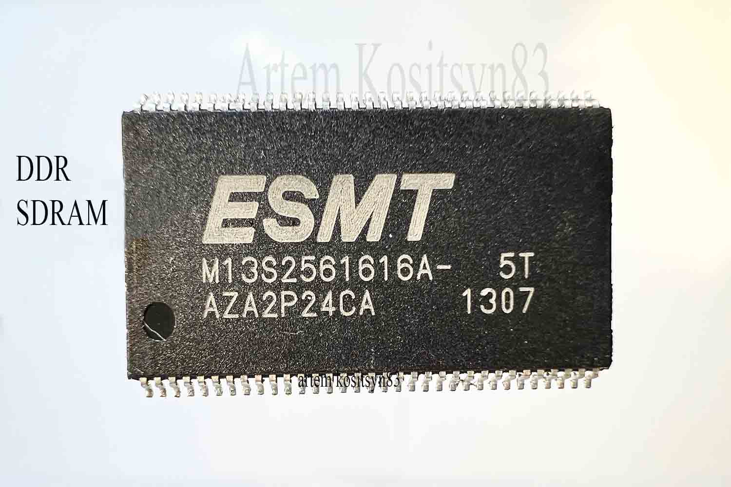
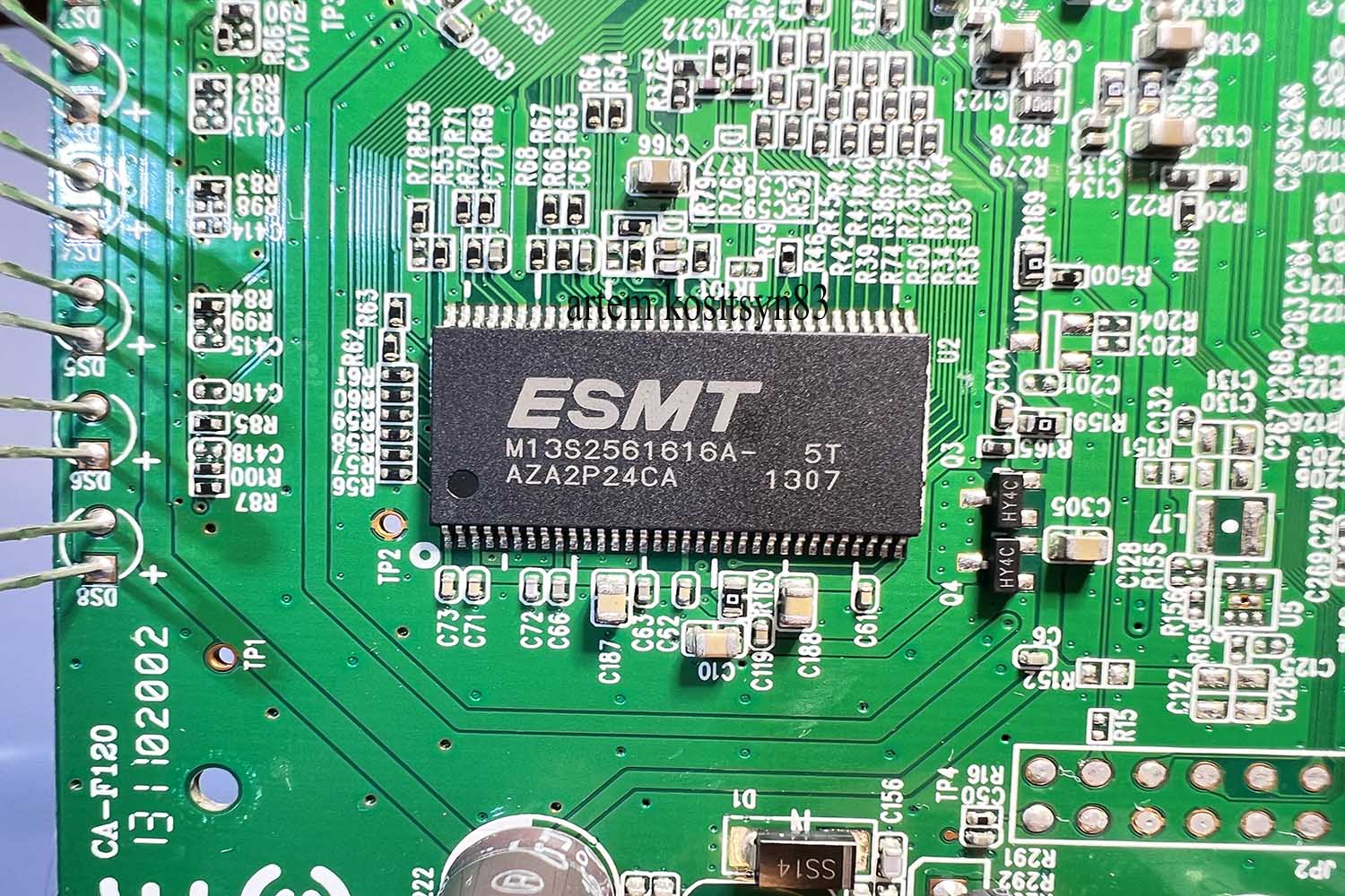
M13S2561616A 4M x 16 Bit x 4 Banks Double Data Rate SDRAM
–Double-data-rate architecture, two data transfers per clock cycle –Bi-directional data strobe (DQS) –Differential clock inputs (CLK and CLK ) –DLL aligns DQ and DQS transition with CLK transition –Four bank operation –CAS Latency : 2.5, 3, 4 –Burst Type : Sequential and Interleave –Burst Length : 2, 4, 8 –All inputs except data & DM are sampled at the rising edge of the system clock (CLK) –Data I/O transitions on both edges of data strobe (DQS) –DQS is edge-aligned with data for READs; center-aligned with data for WRITEs –Data mask (DM) for write masking only –VDD = 2.5V ± 0.2V, VDDQ = 2.5V ± 0.2V –7.8us refresh interval –Auto & Self refresh –2.5V I/O (SSTL_2 compatible)